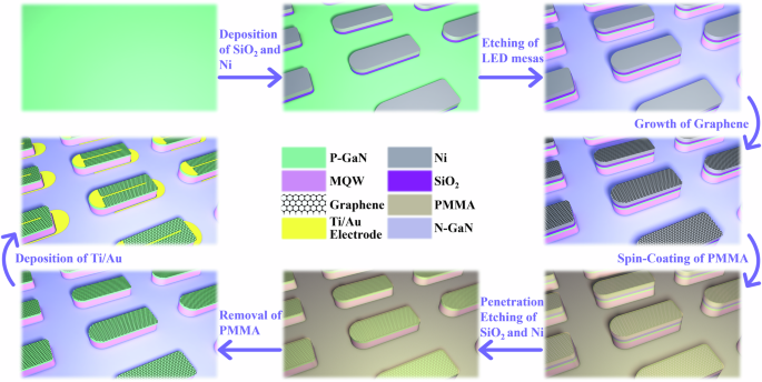
Figure 1 is a schematic diagram of the process flow of a 2-inch wafer-scale LED chip with transfer-free patterned graphene as TEs. Eight of the images show the status of the sample at different stages, and the corresponding process operations…
Wafer-scale transfer-free patterned graphene transparent electrodes for GaN-based LEDs: a universal technique towards different substrates