Free-standing growth of MoO3 dielectrics
The physical vapor deposition (PVD) technique was employed to grow layered MoO3 on SiO2/Si substrates (see Methods for details). From the scanning electron microscopy (SEM) images as shown in Fig. 1a, b,…
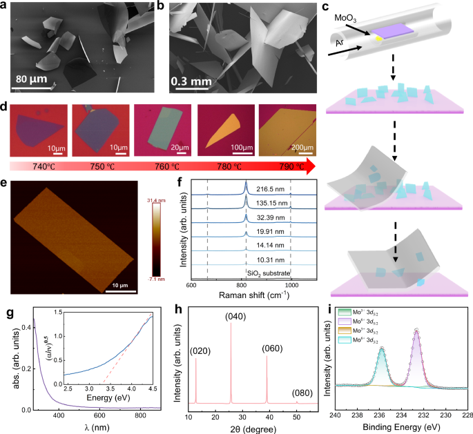
The physical vapor deposition (PVD) technique was employed to grow layered MoO3 on SiO2/Si substrates (see Methods for details). From the scanning electron microscopy (SEM) images as shown in Fig. 1a, b,…